|
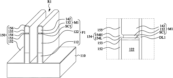
1. A method for manufacturing a semiconductor device, comprising: forming at least one epitaxial layer over a substrate; forming a mask over the epitaxial layer; patterning the epitaxial layer into a semiconductor fin; depositing a conformal semiconductor capping layer over the semiconductor fin and the mask, wherein the conformal semiconductor capping layer has a first portion that is amorphous on a sidewall of the mask and a second portion that is crystalline on a sidewall of the semiconductor fin; performing a thermal treatment such that the first portion of the conformal semiconductor capping layer is converted from amorphous into crystalline; forming an isolation structure around the semiconductor fin; and forming a gate structure over the semiconductor fin.
|