| CPC H01L 21/76224 (2013.01) [H01L 21/31053 (2013.01); H01L 27/10 (2013.01)] | 12 Claims |
|
1. A method for forming a shallow trench isolation structure with reduced encroachment of active regions of a silicon substrate, comprising:
providing a silicon substrate;
forming a pad oxide layer on an upper surface of the silicon substrate;
forming a silicon nitride layer on the pad oxide layer;
forming a first pattern on the silicon nitride layer, wherein the first pattern is composed of lines aligned in rows along a first dimension, or the first pattern is composed of a first sub-pattern and a second sub-pattern, wherein the first sub-pattern is composed of lines aligned in rows along a first dimension and the second sub-pattern contains openings with one or more sizes aligned in rows along the first dimension;
using the first pattern as a mask and performing a first trench etching process to form a plurality of first trenches along the first dimension, wherein the first trenches have one or more sizes;
removing the first pattern;
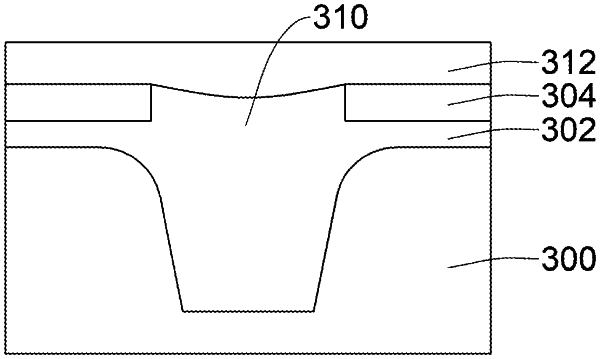
performing a first thermal oxidation process to form a first liner oxide on sidewalls and bottoms of the first trenches;
filling the first trenches with a first dielectric material;
forming a second pattern with active-area-defined portions on the silicon substrate, wherein the active-area-defined portions have one or more sizes;
using the second pattern as a mask and performing a second trench etching process to form a plurality of second trenches in a second dimension to define a plurality of the active regions of the silicon substrate, and the active regions are separated from each other by the first trenches filled with the first dielectric material and the second trenches, wherein the active regions has one or more sizes and the second trenches have one or more sizes;
performing a second thermal oxidation process to form a second liner oxide on sidewalls and bottoms of the second trenches; and
filing the second trenches with a second dielectric material.
|