| CPC H01L 21/56 (2013.01) [H01L 21/568 (2013.01); H01L 21/6835 (2013.01); H01L 23/13 (2013.01); H01L 23/3128 (2013.01); H01L 23/49816 (2013.01); H01L 23/49827 (2013.01); H01L 24/81 (2013.01); H01L 24/92 (2013.01); H01L 24/94 (2013.01); H01L 24/97 (2013.01); H01L 25/0657 (2013.01); H01L 25/105 (2013.01); H01L 25/16 (2013.01); H01L 23/552 (2013.01); H01L 24/16 (2013.01); H01L 24/29 (2013.01); H01L 24/32 (2013.01); H01L 24/48 (2013.01); H01L 24/83 (2013.01); H01L 2221/68345 (2013.01); H01L 2224/0401 (2013.01); H01L 2224/04105 (2013.01); H01L 2224/0557 (2013.01); H01L 2224/05552 (2013.01); H01L 2224/12105 (2013.01); H01L 2224/16145 (2013.01); H01L 2224/16146 (2013.01); H01L 2224/16225 (2013.01); H01L 2224/16227 (2013.01); H01L 2224/32145 (2013.01); H01L 2224/45015 (2013.01); H01L 2224/4816 (2013.01); H01L 2224/48091 (2013.01); H01L 2224/48157 (2013.01); H01L 2224/48158 (2013.01); H01L 2224/73203 (2013.01); H01L 2224/73253 (2013.01); H01L 2224/73259 (2013.01); H01L 2224/73265 (2013.01); H01L 2224/73267 (2013.01); H01L 2224/81001 (2013.01); H01L 2224/812 (2013.01); H01L 2224/81801 (2013.01); H01L 2224/83 (2013.01); H01L 2224/97 (2013.01); H01L 2225/06513 (2013.01); H01L 2225/06517 (2013.01); H01L 2225/06541 (2013.01); H01L 2225/06548 (2013.01); H01L 2225/06589 (2013.01); H01L 2924/0002 (2013.01); H01L 2924/00014 (2013.01); H01L 2924/0103 (2013.01); H01L 2924/014 (2013.01); H01L 2924/01004 (2013.01); H01L 2924/01005 (2013.01); H01L 2924/0105 (2013.01); H01L 2924/01006 (2013.01); H01L 2924/01013 (2013.01); H01L 2924/01019 (2013.01); H01L 2924/01029 (2013.01); H01L 2924/01047 (2013.01); H01L 2924/01049 (2013.01); H01L 2924/01073 (2013.01); H01L 2924/01074 (2013.01); H01L 2924/01078 (2013.01); H01L 2924/01079 (2013.01); H01L 2924/01082 (2013.01); H01L 2924/01322 (2013.01); H01L 2924/09701 (2013.01); H01L 2924/12041 (2013.01); H01L 2924/12042 (2013.01); H01L 2924/12044 (2013.01); H01L 2924/1306 (2013.01); H01L 2924/13091 (2013.01); H01L 2924/14 (2013.01); H01L 2924/157 (2013.01); H01L 2924/1532 (2013.01); H01L 2924/15151 (2013.01); H01L 2924/15174 (2013.01); H01L 2924/15311 (2013.01); H01L 2924/15331 (2013.01); H01L 2924/181 (2013.01); H01L 2924/18161 (2013.01); H01L 2924/19041 (2013.01); H01L 2924/19105 (2013.01); H01L 2924/207 (2013.01); H01L 2924/3025 (2013.01); H01L 2924/30105 (2013.01); H01L 2924/3511 (2013.01)] | 21 Claims |

|
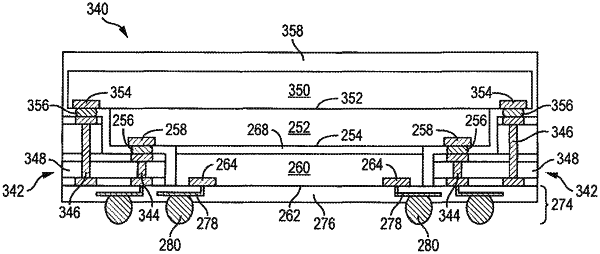
1. A semiconductor device, comprising:
a stepped substrate including a first layer and a second layer disposed over the first layer, wherein the stepped substrate comprises a first surface, a first step level at a surface of the first layer opposite the first surface, and a second step level at a surface of the second layer offset from the first step level;
a first semiconductor die disposed in an opening of the stepped substrate;
a second semiconductor die disposed over the first step level;
a first conductive via formed through the stepped substrate;
a third semiconductor die disposed over the second step level with a surface of the third semiconductor die in contact with a surface of the second semiconductor die;
an encapsulant deposited around the first semiconductor die, around the second semiconductor die, over the third semiconductor die, and over the stepped substrate; and
a build-up interconnect structure formed on an active surface of the first semiconductor die opposite the second semiconductor die, and on the first surface of the stepped substrate, wherein the build-up interconnect structure includes,
(a) an insulating layer formed on the active surface of the first semiconductor die, and on the first surface of the stepped substrate, and
(b) a conductive layer formed on the insulating layer and on the active surface of the first semiconductor die.
|