| CPC H01L 21/31155 (2013.01) [H01J 37/3171 (2013.01); H01J 2237/3171 (2013.01)] | 20 Claims |
|
1. A method for forming a semiconductor structure, comprising:
forming a pattern comprising a first line feature and a second line feature extending in a first direction on a substrate;
depositing a photoresist layer on the substrate to cover the pattern;
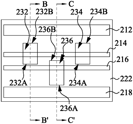
patterning the photoresist layer to form a cut pattern comprising a first cut feature exposing a portion of the first line feature and a second cut feature exposing a portion of the second line feature, wherein in a top view, at least one of the first cut feature and the second cut feature is asymmetrically arranged with respect to a central axis of a corresponding first or second line feature;
performing at least one angled ion implantation to enlarge the first cut feature and the second cut feature in at least one direction perpendicular to the first direction;
removing the portion of the first line feature exposed by the first cut feature and the portion of the second line feature exposed by the second cut feature; and
removing the photoresist layer.
|
|
7. A method for forming a semiconductor structure, comprising:
forming a pattern on a substrate, wherein the pattern comprises a first line feature and a second line feature extending in a first direction;
depositing a photoresist layer on the substrate to cover the pattern;
patterning the photoresist layer to form a first cut feature exposing a portion of the first line feature and a second cut feature exposing a portion of the second line feature, wherein in a top view, the first cut feature is asymmetrically arranged with respect to a central axis of the first line feature;
performing a first angled ion implantation to enlarge the first cut feature and the second cut feature in a second direction perpendicular to the first direction;
removing the portion of the first line feature exposed by the first cut feature and the portion of the second line feature exposed by the second cut feature; and
removing the photoresist layer.
|
|
16. A method for forming a semiconductor structure, comprising:
etching a patterning-target layer to form a pattern on a substrate, wherein the pattern comprises a first line feature and a second line feature extending in a first direction;
depositing a photoresist layer on the substrate to cover the pattern;
patterning the photoresist layer to form a first cut feature exposing a portion of the first line feature and a second cut feature exposing a portion of the second line feature, wherein each of the first cut feature and the second cut features has first and second sidewalls extending in the first direction, a first spacing between the first sidewall of the first cut feature and the first line feature is greater than a second spacing between the second sidewall of the first cut feature and the first line feature, a first spacing between the first sidewall of the second cut feature and the second line feature is less than a second spacing between the second sidewall of the second cut feature and the second line feature, the second sidewall of the first cut feature is proximate to the second line feature, and the first sidewall of the second cut feature is proximate to the first line feature;
performing a first angled ion implantation to enlarge the first cut feature and the second cut feature in a second direction perpendicular to the first direction;
performing a second angled ion implantation to enlarge the first cut feature and the second cut feature in a third direction opposite the second direction;
removing the portion of the first line feature exposed by the first cut feature and the portion of the second line feature exposed by the second cut feature; and
removing the photoresist layer.
|