| CPC H01C 1/142 (2013.01) [H01C 7/003 (2013.01)] | 17 Claims |
|
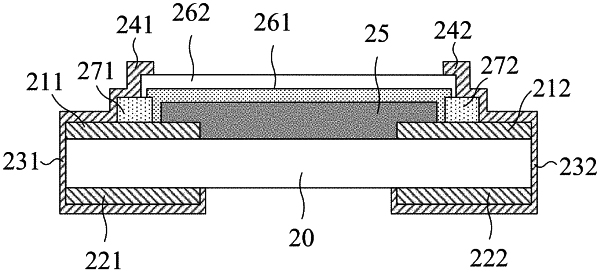
1. A chip resistor structure, comprising:
a substrate;
a pair of first electrodes disposed opposite to each other on a first surface of the substrate at a first interval;
a resistance layer disposed between the pair of first electrodes on the first surface, and having two opposite ends extending over the pair of first electrodes, respectively;
a spacer layer made of a material having a composition different from that of the resistance layer, disposed over the pair of first electrodes, and including a first portion and a second portion extending from the pair of first electrodes over the two opposite ends of the resistance layer, respectively, wherein a length of the second portion is in a range of 12% to 21% length of the chip resistor structure, and each of the first portion and the second portion of the spacer layer has a first width less than a width of the resistance layer covered thereby;
a protective layer overlying the resistance layer; and
a plating layer electroplated onto the pair of first electrodes and the spacer layer, and having ends extending beyond the pair of first electrodes terminate at least over the spacer layer.
|