| CPC G11C 11/54 (2013.01) [G06N 3/065 (2023.01); G06N 3/08 (2013.01); G11C 11/221 (2013.01); H10B 53/30 (2023.02); H10B 53/40 (2023.02)] | 3 Claims |
|
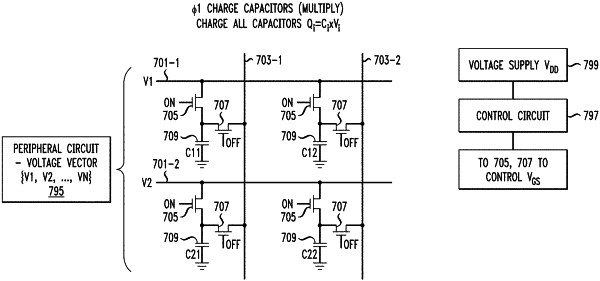
1. An electronic circuit, comprising:
a plurality of word lines;
a plurality of bit lines intersecting said plurality of word lines at a plurality of grid points;
a plurality of integrators coupled to said plurality of bit lines;
a voltage vector peripheral circuit;
a voltage supply;
a control circuit; and
a plurality of in-memory processing cells located at said plurality of grid points, each of said in-memory processing cells comprising:
a first switch having a first terminal coupled to a corresponding one of said word lines and a second terminal;
a second switch having a first terminal coupled to said second terminal of said first switch and a second terminal coupled to a corresponding one of said bit lines, wherein said first switch and said second switch both are field effect transistors of a same type that is selected from the list consisting of: NMOS and PMOS; and
a non-volatile tunable capacitor having one electrode coupled to said second terminal of said first switch and said first terminal of said second switch, and having another electrode coupled to ground,
wherein said voltage vector peripheral circuit, said voltage supply, and said control circuit are cooperatively configured to:
in a multiply phase, close said first switches, open said second switches, and apply a voltage vector from said voltage vector peripheral circuit to said word lines; and
in an accumulate phase, open said first switches, and close said second switches to connect, to a corresponding one of said integrators, each of said non-volatile tunable capacitors that is associated with a given one of said bit lines.
|