| CPC G11C 11/40615 (2013.01) [G11C 11/4087 (2013.01); G11C 11/4093 (2013.01); G11C 11/40622 (2013.01); G11C 29/4401 (2013.01)] | 20 Claims |
|
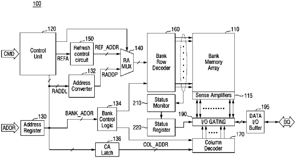
1. A memory device comprising:
a bank memory array including memory cells;
a control unit configured to indicate a target row of the bank memory array in response to a refresh command received from an external source;
a refresh control circuit that provides a refresh row address in response to the control unit indicating the target row;
a row decoder that applies a refresh drive voltage to the refresh row address;
a status monitor that monitors row-specific status information for memory cells of the target row;
a status register that stores the status information under control of the status monitor; and
a data input/output (I/O) buffer that receives the status information from the status register and provides the status information to the external source in response to the refresh command.
|