| CPC G11C 11/404 (2013.01) | 10 Claims |
|
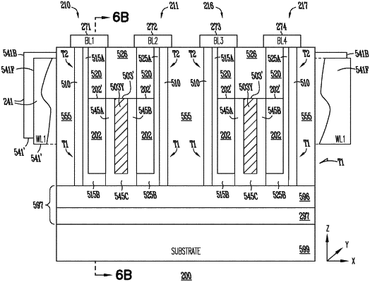
1. An apparatus comprising:
a first data line;
a second data line;
a conductive region;
a first memory cell including a first transistor and a second transistor, the first transistor including a first channel region coupled between the first data line and the conductive region, and a first charge storage structure located between the first data line and the conductive region, the second transistor including a second channel region coupled to and located between the first data line and the first charge storage structure;
a second memory cell including a third transistor and a fourth transistor, the third transistor including a third channel region coupled between the second data line and the conductive region, and a second charge storage structure located between the second data line and the conductive region, the fourth transistor including a fourth channel region coupled to and located between the second data line and the second charge storage structure;
a conductive line forming a gate of each of the first, second, third, and fourth transistors; and
a conductive structure located between the first and second charge storage structures and electrically separated from the conductive region.
|