US 11,688,445 B2
Valley spin hall effect based non-volatile memory
Sandeep Krishna Thirumala, West Lafayette, IN (US); Sumeet Kumar Gupta, West Lafayette, IN (US); Yi-Tse Hung, New Taipei (TW); and Zhihong Chen, West Lafayette, IN (US)
Assigned to Purdue Research Foundation, West Lafayette, IN (US)
Filed by Purdue Research Foundation, West Lafayette, IN (US)
Filed on Jan. 30, 2022, as Appl. No. 17/588,317.
Application 17/588,317 is a continuation of application No. 16/909,971, filed on Jun. 23, 2020, granted, now 11,250,896.
Claims priority of provisional application 62/865,280, filed on Jun. 23, 2019.
Prior Publication US 2022/0157359 A1, May 19, 2022
This patent is subject to a terminal disclaimer.
Int. Cl. G11C 11/00 (2006.01); G11C 11/16 (2006.01); G11C 11/18 (2006.01); H10B 61/00 (2023.01); H10N 52/80 (2023.01); H10N 52/00 (2023.01)
CPC G11C 11/161 (2013.01) [G11C 11/1673 (2013.01); G11C 11/1675 (2013.01); G11C 11/18 (2013.01); H10B 61/00 (2023.02); H10N 52/101 (2023.02); H10N 52/80 (2023.02)] 19 Claims
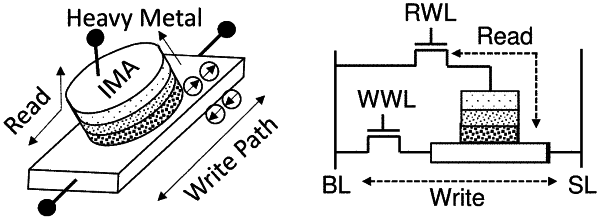
OG exemplary drawing
 
1. A memory cell, comprising:
a semiconductor layer;
a first electrode coupled to the semiconductor layer;
a second electrode coupled to the semiconductor layer, wherein the first and second electrodes are separated from one another along a first axis and wherein the semiconductor layer extends beyond the first axis along a second axis substantially perpendicular to the first axis, thereby forming a first wing;
a third electrode separated from the semiconductor layer by an insulating layer;
a first magnetic tunnel junction (MTJ) disposed on the first wing; and
a first read electrode coupled to the first MTJ.