| CPC G11C 7/12 (2013.01) [G11C 7/106 (2013.01); G11C 7/1048 (2013.01); G11C 7/1057 (2013.01); G11C 7/1084 (2013.01); G11C 7/1087 (2013.01)] | 11 Claims |
|
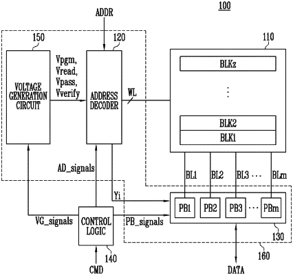
1. A page buffer comprising:
a bit line selector configured to connect a bit line of a memory cell array to a sensing node;
a precharger configured to precharge a potential of the sensing node to a first level; and
a latch component configured to sense data by detecting a time at which the potential of the sensing node is decreased from the first level to a second level,
wherein the latch component comprises:
a first latch stage configured to latch data corresponding to the potential of the sensing node in response to a rising edge of a latch signal and configured to output the latched data to a first output terminal in response to a falling edge of the latch signal;
a second latch stage configured to latch the data that is received from the first output terminal in response to the rising edge of the latch signal and configured to output the latched data to a second output terminal in response to the falling edge of the latch signal; and
a third latch stage configured to latch the data that is received from the second output terminal in response to the rising edge of the latch signal and configured to output the latched data to a third output terminal in response to the falling edge of the latch signal.
|