| CPC G09G 3/3258 (2013.01) [G09G 2300/0426 (2013.01); G09G 2300/0842 (2013.01); G09G 2310/061 (2013.01)] | 20 Claims |
|
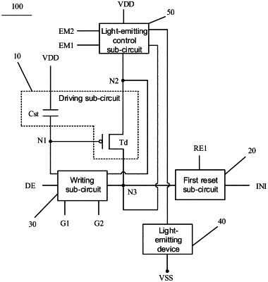
1. A pixel circuit, comprising:
a driving sub-circuit, the driving sub-circuit including:
a driving transistor, a gate of the driving transistor being connected to a first node, a first electrode of the driving transistor being connected to a second node, and a second electrode of the driving transistor being connected to a third node; and
a storage capacitor, including a first storage electrode and a second storage electrode, the first storage electrode being connected to the first node, and the second storage electrode being connected to a first voltage terminal;
a first reset sub-circuit connected to at least the third node, a first reset signal terminal and an initialization signal terminal; the first reset sub-circuit being configured to, in an initialization phase, transmit an initialization signal from the initialization signal terminal to the third node under control of at least a first reset signal received at the first reset signal terminal;
a writing sub-circuit connected to a first scanning terminal, a second scanning terminal, a data terminal, the first node, the second node, and the third node; the writing sub-circuit being configured to: in the initialization phase, transmit the initialization signal at the third node to the first node under control of a first scanning signal received at the first scanning terminal, so as to reset the first node; and in a data writing phase, write a data signal received at the data terminal to the first node and perform threshold voltage compensation on the driving transistor under the control of the first scanning signal received at the first scanning terminal and control of a second scanning signal received at the second scanning terminal;
a light-emitting device including an anode and a cathode, the cathode being connected to a second voltage terminal; and
a light-emitting control sub-circuit connected to the second node, the third node, the first voltage terminal, a first enable signal terminal, a second enable signal terminal, and the anode of the light-emitting device; the light-emitting control sub-circuit being configured to: in a light-emitting phase, under control of a first enable signal received at the first enable signal terminal and control of a second enable signal received at the second enable signal terminal, transmit a voltage signal of the first voltage terminal to the second node, and transmit a current output by the driving transistor to the light-emitting device to make the light-emitting device emit light.
|