| CPC G09G 3/3233 (2013.01) [G09G 3/3266 (2013.01); G09G 3/3283 (2013.01); G09G 2300/0426 (2013.01); G09G 2310/062 (2013.01); G09G 2320/0233 (2013.01); G09G 2320/0626 (2013.01); H01L 29/78693 (2013.01); H10K 59/1213 (2023.02)] | 18 Claims |
|
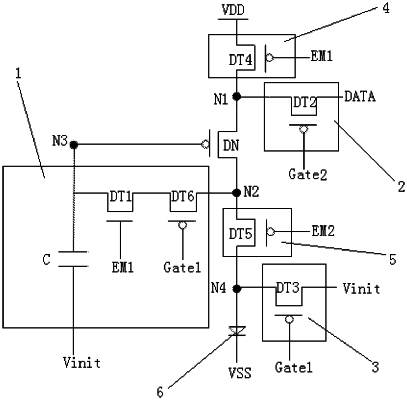
1. A pixel driving circuit, comprising a driving transistor, a storage sub-circuit, a data writing sub-circuit, a first light-emission control sub-circuit, a second light-emission control sub-circuit and a light-emitting element, wherein:
the data writing sub-circuit is connected to the driving transistor, and is configured to write a data signal to the driving transistor in response to a second scan signal;
the storage sub-circuit is connected to a gate electrode of the driving transistor, a second electrode of the driving transistor and an initial voltage terminal, and is configured to store the data signal written by the data writing sub-circuit;
the first light-emission control sub-circuit is connected to a first electrode of the driving transistor and a first power terminal, and is configured to apply a voltage of the first power terminal to the first electrode of the driving transistor in response to a first light-emission signal;
the driving transistor is configured to generate a drive current in response to the data signal stored in the gate electrode of the driving transistor by the storage sub-circuit, and under action of the voltage applied to the first electrode of the driving transistor by the first light-emission control sub-circuit; and
the second light-emission control sub-circuit is connected to the second electrode of the driving transistor and a first end of the light-emitting element, and is configured to apply the drive current to the light-emitting element in response to a second light-emission signal, wherein a second end of the light-emitting element is connected to a second power terminal,
wherein the initial voltage terminal is configured to provide a reset voltage, the first power terminal is configured to provide a first power voltage, and the second power terminal is configured to provide a second power voltage,
wherein: the storage sub-circuit comprises a storage capacitor and a first transistor, a first end of the storage capacitor is connected to the gate electrode of the driving transistor, and a second end of the storage capacitor is directly connected to the initial voltage terminal; and
a gate electrode of the first transistor is connected to a first light-emission control line that provides the first light-emission signal, a first electrode of the first transistor is connected to the first end of the storage capacitor, and a second electrode of the first transistor is connected to the second electrode of the driving transistor,
wherein: the first light-emission control sub-circuit comprises a fourth transistor, and the second light-emission control circuit comprises a fifth transistor;
a gate electrode of the fourth transistor is connected to the first light-emission control line, a first electrode of the fourth transistor is connected to the first power terminal, and a second electrode of the fourth transistor is connected to the first electrode of the driving transistor; and
a gate electrode of the fifth transistor is connected to a second light-emission control line that provides the second light-emission signal, a first electrode of the fifth transistor is connected to the second electrode of the driving transistor, and a second electrode of the fifth transistor is connected to the first end of the light-emitting element.
|