| CPC G09G 3/3225 (2013.01) [G11C 19/28 (2013.01); H01L 27/3276 (2013.01); G09G 3/3266 (2013.01); G09G 2300/0426 (2013.01); G09G 2310/0286 (2013.01); G09G 2310/08 (2013.01); G09G 2330/02 (2013.01); G09G 2330/08 (2013.01)] | 20 Claims |
|
1. A display substrate, comprising: a base substrate, and a shift register unit and a first clock signal line that are on the base substrate,
wherein the first clock signal line extends along a first direction on the base substrate and is configured to provide a first clock signal to the shift register unit;
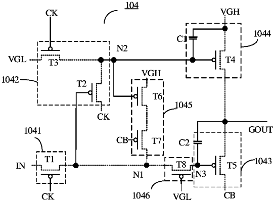
the shift register unit comprises an input circuit, an output circuit, a first control circuit and an output control circuit;
the input circuit is configured to input an input signal to a first node in response to the first clock signal;
the output circuit is configured to output an output signal to an output terminal;
the first control circuit is configured to control a level of a second node in response to a level of the first node and the first clock signal;
the output control circuit is configured to control a level of the output terminal under control of the level of the second node,
wherein the first control circuit comprises a first control transistor and a second control transistor,
an active layer of the first control transistor and an active layer of the second control transistor are a continuous control semiconductor layer, the control semiconductor layer extends along the first direction, and a gate electrode of the first control transistor and a gate electrode of the second control transistor extend along a second direction different from the first direction and are arranged side by side in the first direction.
|