| CPC G09G 3/32 (2013.01) [G11C 19/28 (2013.01); H01L 25/0753 (2013.01); H01L 27/0296 (2013.01); H01L 27/124 (2013.01); H01L 33/62 (2013.01); G09G 2300/026 (2013.01); G09G 2310/0286 (2013.01); G09G 2330/04 (2013.01)] | 20 Claims |
|
1. An array substrate, having a display area, the array substrate comprising:
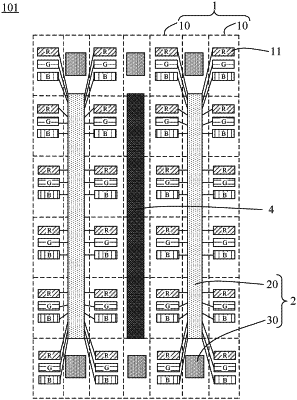
at least one pixel group disposed in the display area, each pixel group including a plurality of pixels, each of the plurality of pixels including at least one sub-pixel; and
at least one pixel circuit group; wherein
the at least one pixel group includes at least two pixel groups;
the at least two pixel groups are arranged in a row direction; a pixel circuit group of the at least one pixel circuit group is electrically connected to two adjacent pixel groups arranged in the row direction, and is located between two adjacent columns of sub-pixels belonging to different pixel groups in the two adjacent pixel groups; in a column direction, a length of a pixel group of the at least two pixel groups arranged in the row direction is greater than a length of a pixel circuit group electrically connected thereto; and an orthographic projection, on a plane, of a sub-pixel in the at least two pixel groups arranged in the row direction does not overlap with an orthographic projection, on the plane, of a pixel circuit group electrically connected to a pixel group to which the sub-pixel in the at least two pixel groups arranged in the row direction belongs, the plane being perpendicular to the column direction; or
the at least two pixel groups are arranged in the column direction; a pixel circuit group of the at least one pixel circuit group is electrically connected to two adjacent pixel groups arranged in the column direction, and is located between two adjacent rows of sub-pixels belonging to different pixel groups in the two adjacent pixel groups; in the row direction, a length of a pixel group of the at least two pixel groups arranged in the column direction is greater than a length of a pixel circuit group electrically connected thereto; and an orthographic projection, on another plane, of a sub-pixel in the at least two pixel groups arranged in the column direction does not overlap with an orthographic projection, on the another plane, of a pixel circuit group electrically connected to a pixel group to which the sub-pixel in the at least two pixel groups arranged in the column direction belongs, the another plane being perpendicular to the row direction.
|