| CPC G06F 11/1004 (2013.01) [G06F 11/1068 (2013.01); G06F 13/1668 (2013.01); H04B 1/04 (2013.01)] | 16 Claims |
|
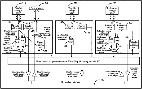
1. A data transmission circuit, wherein the data transmission circuit comprises:
a normal reading module, which is connected to a normal storage array, and is configured to read and output data from the normal storage array;
a redundant reading module, which is connected to a redundant storage array, and is configured to read and output data from the redundant storage array; and
an error detection operation module, which is connected to the normal reading module and the redundant reading module respectively, and is configured to synchronously receive the read data output from the normal reading module and the redundant reading module, and perform an error detection operation on the read data.
|