| CPC G06F 3/0655 (2013.01) [G06F 3/0619 (2013.01); G06F 3/0679 (2013.01)] | 34 Claims |
|
1. A method, comprising:
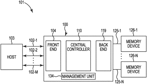
receiving a first signal indicative of data from a host by interface management circuitry of a memory controller configured for a Compute Express Link (CXL) protocol;
generating error detection information based on the data by data management circuitry of the memory controller;
generating error correction information based on the data by the data management circuitry;
transmitting a second signal indicative of the data to a memory device by a plurality of data pins of a memory interface of the memory controller configured for a low-power double data rate (LPDDRx) protocol;
transmitting a third signal indicative of the error detection information and the error correction information to the memory device by a plurality of data mask inversion (DMI) pins of the memory interface of the memory controller configured for LPDDRx protocol contemporaneous with the transmission of the data; and
prohibiting, by firmware, enablement of a dynamic voltage frequency scaling core (DVFSC) of the memory device.
|