| CPC G06F 3/0626 (2013.01) [G06F 3/065 (2013.01); G06F 3/0611 (2013.01); G06F 3/0658 (2013.01); G06F 3/0659 (2013.01); G06F 3/0685 (2013.01)] | 16 Claims |
|
1. A memory system for storing data in response to commands received from a Host that is remote from the memory system, the memory system comprising:
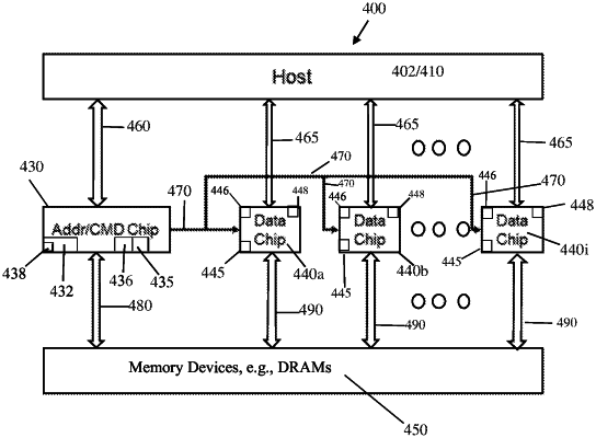
a memory control circuit formed on a single chip and configured to receive commands from the Host;
a plurality of memory devices, each of the plurality of memory devices formed on a single chip, and configured to store data and receive command signals from the memory control circuit;
a plurality of data buffer circuits, each of the plurality of data buffer circuits formed on a separate chip and associated with one of the plurality of memory devices, wherein the at least one of the plurality of data buffer circuits comprises a data buffer state machine-driven local address sequencer that has a pointer that identifies the next local store data tag identifying a location of the at least one of the plurality of data buffer circuits to write data, wherein the state machine-driven local address pointer of the at least one of the plurality of data buffer circuits is synchronized with a pointer of a state machine driven local address sequencer of the Host;
a data link for communicating data between the Host and the plurality of memory devices, wherein the data link includes a data communications link directly connecting the Host and each of the plurality of data buffer circuits for sending only data or only data and cyclic redundancy check (CRC) directly between the Host and each of the plurality of data buffer circuits, and a data transfer link directly connecting the plurality of data buffer circuits and the plurality of memory devices for sending the data directly between the plurality of memory devices and the plurality of memory devices;
a communications link directly connecting the Host and the memory control circuit for sending commands from the Host directly to the memory control circuit;
a command bus directly connecting the memory control circuit and the plurality of memory devices; and
a one-way control communications link directly connecting the memory control circuit and the plurality of data buffer circuits and no link connecting the memory control circuit and the plurality of data buffer circuits for transmitting data from the memory control circuit to the plurality of data buffer circuits, wherein the one-way control communications link is for sending commands directly from the memory control circuit to the plurality of data buffer circuits and not sending the data over the one-way control communications link directly connecting the memory control circuit and the plurality of data buffer circuits,
wherein the memory control circuit chip, the plurality of memory chips, the plurality of data buffer chips, the data link, the communications link, the command bus, and the one-way control communications link are configured on a single module where the plurality of memory device chips are arranged in groups,
wherein the memory control circuit is configured to:
receive a store command and a local store data tag from the Host over the communications link directly connecting the Host and the memory control circuit, wherein the local store data tag specifies a location in the plurality of data buffer circuits;
in response to receiving the Host store command, decode the store command into a write-to-buffer command for writing data from the Host to the plurality of data buffer circuits and a store-from-buffer command for storing data from the plurality of data buffer circuits to the plurality of memory chips; and
send the write-to-buffer command to at least one of the plurality of data buffer circuits over the one-way control communications link, but not send the local store data tag together with the write-to-buffer command over the one-way control communications link to the at least one of the plurality of data buffer circuits, and
wherein the at least one of the plurality of data buffer circuits is configured to:
not receive the local store data tag specifying the location to store the data in the at least one of the plurality of data buffer circuits.
|