| CPC G06F 3/04164 (2019.05) [G02F 1/1368 (2013.01); G02F 1/13338 (2013.01); G02F 1/134309 (2013.01); G02F 1/136286 (2013.01); G06F 3/0412 (2013.01); H01L 27/124 (2013.01); G09G 2300/08 (2013.01); H01L 27/1248 (2013.01)] | 20 Claims |
|
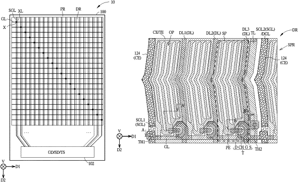
1. A touch display device, having a display region and a peripheral region, the touch display device comprising:
a substrate;
a first metal layer disposed on the substrate, wherein the first metal layer comprises a scan line and a gate of a thin film transistor;
a first insulating layer disposed on the first metal layer;
a second metal layer disposed on the first insulating layer, wherein the second metal layer comprises a data line, a touch signal line and a source and a drain of the thin film transistor;
a first transparent conductive layer disposed on the first insulating layer, wherein the first transparent conductive layer comprises a pixel electrode, and the pixel electrode is electrically connected to the drain of the thin film transistor;
a second insulating layer and a third insulating layer disposed on the second metal layer and the first transparent conductive layer, wherein the third insulating layer is disposed on the second insulating layer;
a third metal layer disposed between the second insulating layer and the third insulating layer, wherein the third metal layer comprises a scan signal line; and
a second transparent conductive layer disposed on the third insulating layer, wherein the second transparent conductive layer comprises a touch electrode,
wherein
the scan line and the data line are disposed on the substrate, and an extending direction of the scan line in the display region is different from an extending direction of the data line in the display region;
the thin film transistor is disposed on the substrate and in the display region, the scan line is electrically connected to the gate of the thin film transistor, and the data line is electrically connected to the source of the thin film transistor;
the scan signal line is disposed on the substrate, an extending direction of the scan signal line in the display region is different from the extending direction of the scan line in the display region, and the scan signal line is electrically connected to the scan line; and
the touch signal line and the touch electrode are disposed on the substrate, and the touch signal line is electrically connected to the touch electrode.
|