| CPC G06F 1/3253 (2013.01) [G06F 13/4068 (2013.01); G06F 13/4086 (2013.01); G06F 1/266 (2013.01)] | 19 Claims |

|
1. An interface circuit, comprising:
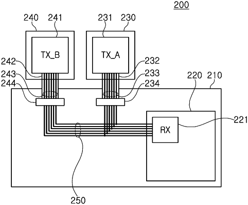
a first transmission circuit configured to output a first signal to a transmission line via first transfer pads; and
a second transmission circuit configured to output a second signal to the transmission line via second transfer pads,
wherein the first transmission circuit includes a first termination resistor block including a first switch and a first termination resistor connected in series between the first transfer pads,
wherein the second transmission circuit includes a second termination resistor block including a second switch and a second termination resistor connected in series between the second transfer pads,
wherein, during a first time period, the first transmission circuit is enabled to transmit data and outputs the first signal in a first mode, and during the first time period, the second transmission circuit has a high output impedance, and the second termination resistor block detects the first signal output from the first transmission circuit, and in response to the detection of the first signal, the second terminal resistor block connects the second termination resistor between the second transfer pads such that during a second time period after the first time period, the output impedance of the second transmission circuit has a designated impedance,
wherein, during the second time period, the first transmission circuit outputs data in a second mode, and the second termination resistor block performs impedance matching on the data output from the first transmission circuit, and
wherein the first mode is a mode in which less power is consumed compared to the second mode, and the second mode is a mode in which data is transmitted at a faster speed compared to the first mode.
|