| CPC G06F 1/06 (2013.01) [G06F 13/4022 (2013.01); G11C 11/403 (2013.01); G11C 11/40607 (2013.01)] | 20 Claims |
|
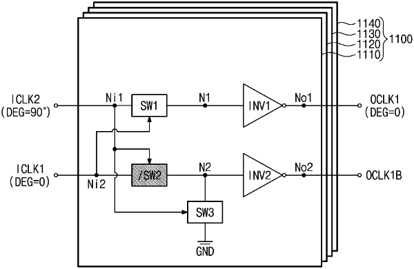
1. A clock converting circuit comprising:
a first switch directly connected between a first input node and a first node, and configured to operate in response to a first logic state of a first input clock, the first input node directly receiving a second input clock delayed with respect to the first input clock by 90 degrees;
a second switch directly connected between a second input node and a second node, and configured to operate in response to a second logic state of the second input clock, the second input node directly receiving the first input clock; and
a third switch connected between the second node and a ground node and configured to operate in response to a first logic state of the second input clock opposite to the second logic state of the second input clock.
|