| CPC G05F 1/56 (2013.01) [G05F 1/44 (2013.01); H03K 17/063 (2013.01); H03K 17/6871 (2013.01); H03K 19/0944 (2013.01)] | 7 Claims |
|
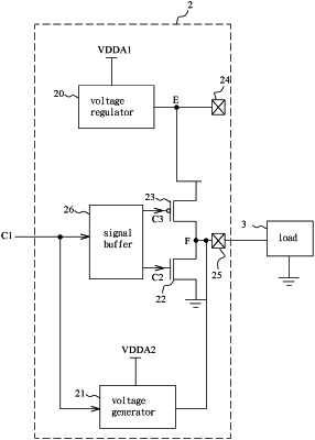
1. A driving device, comprising:
a voltage regulator coupled between a first high-voltage terminal and an output terminal of the driving device and configured to receive a first high voltage of the first high-voltage terminal, wherein the voltage regulator is configured to step down the first high voltage to generate a supply voltage;
a voltage generator coupled to a second high-voltage terminal and the output terminal of the driving device and configured to provide a reference voltage for the output terminal of the driving device, wherein the reference voltage is substantially lower than the supply voltage; and
a first N-channel metal-oxide-semiconductor field effect transistor (NMOSFET) coupled between the output terminal of the driving device and a low-voltage terminal;
wherein the voltage generator includes:
a second N-channel metal-oxide-semiconductor field effect transistor (NMOSFET) coupled to the second high-voltage terminal and the voltage regulator;
a third N-channel metal-oxide-semiconductor field effect transistor (NMOSFET) coupled to the second high-voltage terminal and the output terminal of the driving device;
a first electronic switch coupled between the second NMOSFET and the third NMOSFET;
a fourth N-channel metal-oxide-semiconductor field effect transistor (NMOSFET) coupled to the output terminal of the driving device, the third NMOSFET, and the low-voltage terminal;
a second electronic switch coupled between the fourth NMOSFET and a high bias terminal; and
a signal controller coupled to control terminals of the first electronic switch and the second electronic switch.
|