| CPC G02F 1/134345 (2021.01) [G02B 6/0031 (2013.01); G02B 6/0038 (2013.01); G02F 1/133512 (2013.01)] | 17 Claims |
|
1. A display panel, comprising:
a first substrate and a second substrate;
a liquid crystal layer located between the first substrate and the second substrate;
pixel electrodes located on a side of the first substrate proximate to the liquid crystal layer; and
a light-shielding pattern located on a side of the second substrate proximate to the liquid crystal layer, wherein
the second substrate has a light-shielding region shielded by the light-shielding pattern and light-exiting regions not shielded by the light-shielding pattern;
a pixel electrode in the pixel electrodes is configured to converge light that enters the pixel electrode from the first substrate; and the pixel electrode is used to control a deflection state of a liquid crystal in the liquid crystal layer, so that light passing through the pixel electrode is incident to the light-shielding pattern and/or a corresponding light-exiting region;
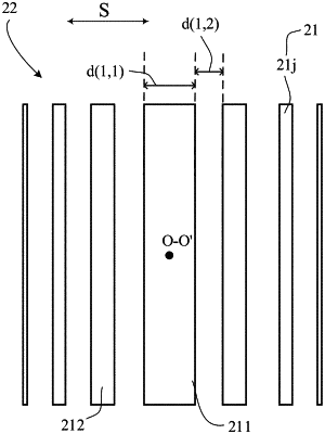
wherein the display panel has a plurality of sub-pixel units, and the pixel electrodes are located in the plurality of sub-pixel units in a one-to-one correspondence;
the pixel electrode includes a plurality of electrode strips arranged in a first direction, and two adjacent electrode strips have a gap therebetween; and
widths of the plurality of electrode strips in the first direction gradually decrease from a center of the pixel electrode to edges of the pixel electrode;
wherein gaps between adjacent electrode strips of the pixel electrode are gradually widened from the center of the pixel electrode to the edges of the pixel electrode.
|