US 11,686,892 B2
Combination structures and optical filters and image sensors and camera modules and electronic devices
Mi Jeong Kim, Hwaseong-si (KR); Sookyoung Roh, Hwaseong-si (KR); Seokho Yun, Hwaseong-si (KR); Ilhwan Kim, Yongin-si (KR); Hyung Jun Kim, Suwon-si (KR); and Chung Kun Cho, Suwon-si (KR)
Assigned to Samsung Electronics Co., Ltd., Gyeonggi-do (KR)
Filed by Samsung Electronics Co., Ltd., Suwon-si (KR)
Filed on Feb. 3, 2020, as Appl. No. 16/780,149.
Claims priority of application No. 10-2019-0064346 (KR), filed on May 31, 2019.
Prior Publication US 2020/0379152 A1, Dec. 3, 2020
Int. Cl. G02B 5/22 (2006.01); G02B 5/28 (2006.01); G02B 5/00 (2006.01); B82Y 20/00 (2011.01)
CPC G02B 5/281 (2013.01) [G02B 5/003 (2013.01); B82Y 20/00 (2013.01)] 28 Claims
OG exemplary drawing
 
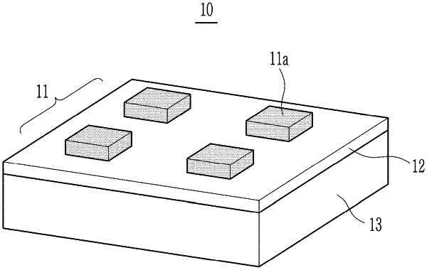
1. A combination structure, comprising
a nanostructure array including a plurality of nanostructures, each of the plurality of nanostructures having a width smaller than a near-infrared wavelength and are repeatedly arranged, and
a light absorption portion adjacent to the nanostructure array, the light absorption portion including a near-infrared absorbing material configured to selectively absorb light in at least a portion of a near-infrared wavelength region.