| CPC G02B 3/0068 (2013.01) [G02B 1/002 (2013.01); G02B 3/0087 (2013.01); H04N 23/55 (2023.01)] | 19 Claims |
|
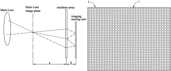
1. A light field imaging device, comprising:
a main lens;
a metalens array which is disposed in alignment with the main lens, wherein the metalens array comprises a plurality of metalenses, and each metalens comprises a plurality of nanostructures and a dielectric layer, the nanostructures are disposed on the dielectric layer, and the nanostructures comprises:
an array of first phase compensation structures, and
an array of second phase compensation structures, wherein the array of the first phase compensation structures are disposed to surround the array of the second phase compensation structures so as to define a single metalens, the first and second phase compensation structures are complementary to each other and substantially satisfy the Babinet's principle; and
an imaging sensing unit which is disposed on an opposite side of the metalens array with respect to the main lens, and is configured to receive an imaging signal generated from the metalens array.
|