| CPC G01V 1/38 (2013.01) [G01S 19/14 (2013.01); G01V 1/164 (2013.01); G01V 1/186 (2013.01)] | 8 Claims |
|
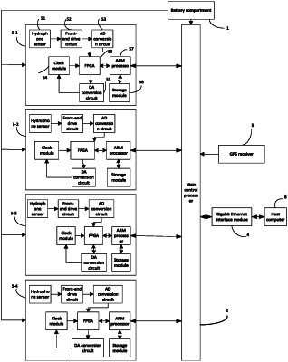
1. A submerged buoy data acquisition system, comprising a battery compartment, a main control processor, a GPS receiver, a gigabit Ethernet interface module, and at least one data acquisition board, wherein the battery compartment is configured to supply power for each electric module, the GPS receiver is connected to an input end of the main control processor, an input end of the gigabit Ethernet interface module is connected to the input end of the main control processor, and an output end of the gigabit Ethernet interface module is connected to a host computer by using a bus;
the data acquisition board comprises a hydrophone sensor, a front-end drive circuit, an AD conversion circuit, a clock module, a DA conversion circuit, an FPGA, an ARM processor, and a storage module, wherein an output end of the hydrophone sensor is connected to an input end of the AD conversion circuit by using the front-end drive circuit, an output end of the AD conversion circuit is connected to an input end of the FPGA, the FPGA is connected to the ARM processor, the storage module is connected to an output end of the ARM processor, an input end of the DA conversion circuit is connected to an output end of the FPGA, an output end of the DA conversion circuit is connected to an input end of the clock module, an output end of the clock module is connected to the input end of the FPGA, and the ARM processor is connected to the main control processor,
the GPS receiver is located on a water's surface;
the front-end drive circuit comprise an analog switch (U2), an operational amplifier (U1) and a differential amplifier (U3); a fifth pin and a seventh pin of the analog switch (U2) are connected to a data signal output end of the hydrophone sensor; a third pin of the analog switch (U2) is connected to a fifth pin of the operational amplifier (U1) by using a resistor (R20) and a resistor (R21) that are connected in series, a ninth pin of the analog switch (U2) is connected to a third pin of the operational amplifier (U1) by using a resistor (R6) and a resistor (R7) that are connected in series, a second pin of the operational amplifier (U1) is grounded by using a resistor (R3); a sixth phi of the operational amplifier (U1) is grounded by using a resistor (R22); a first pin of the operational amplifier (U1) is connected to an eighth pin of the differential amplifier (U3) by using a resistor (R4), a resistor (R5), and a resistor (R8) that are connected in series; a seventh pin of the operational amplifier (U1) is connected to a first pin of the differential amplifier (U3) by using a resistor (R18), a resistor (R19), and a resistor (R15) that are connected in series; a fourth pin of the differential amplifier (U3) is connected to the AD conversion circuit by using a resistor (R16); a fifth pin of the differential amplifier (U3) is connected to the AD conversion circuit by using a resistor (R11).
|