| CPC G01S 7/481 (2013.01) [G01S 7/4815 (2013.01); G01S 7/4816 (2013.01); G01S 17/42 (2013.01); G02B 6/32 (2013.01); G02B 6/4206 (2013.01); G02B 2006/12102 (2013.01)] | 25 Claims |
|
1. A LiDAR system comprising:
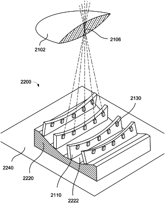
a first optical lens characterized by a first optical axis, a first lens center, and a first surface of best focus;
a first optoelectronic package spaced apart from the first optical lens along the first optical axis, the first optoelectronic package comprising a first plurality of optoelectronic components positioned on a first substrate;
a printed circuit board (PCB), wherein the first optoelectronic package is mounted on the printed circuit board;
a second optoelectronic package mounted on the PCB, the second optoelectronic package comprising:
a second substrate spaced apart from the first optical lens along the first optical axis; and
a second plurality of optoelectronic components positioned on the second substrate, wherein surfaces of respective optoelectronic components of the second plurality of optoelectronic components lie substantially on the first surface of best focus;
an interposer mounting the first optoelectronic package on the PCB, wherein:
the interposer mounts the first optoelectronic package at a different height from the PCB than a height that the second optoelectronic package is mounted from the PCB, so that surfaces of respective optoelectronic components of the first plurality of optoelectronic components lie substantially on the first surface of best focus; and
the first surface of best focus is curved;
a second optical lens characterized by a second optical axis, a second lens center, and a second surface of best focus; and
a third optoelectronic package spaced apart from the second optical lens along the second optical axis, the third optoelectronic package comprising a third plurality of optoelectronic components positioned on a third substrate, separate from the first substrate, such that a surface of each respective optoelectronic component of the third plurality of optoelectronic components lies substantially on the second surface of best focus, wherein the second surface of best focus is curved.
|