| CPC G01R 31/318536 (2013.01) [G01R 31/3177 (2013.01); G01R 31/31723 (2013.01); G01R 31/318544 (2013.01); G01R 31/318583 (2013.01)] | 20 Claims |
|
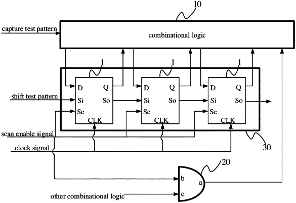
1. A chip, comprising: a combinational logic, a data path gating, and a first scan chain,
wherein the data path gating comprises a first input terminal, a second input terminal, and an output terminal, and the first scan chain is connected to the combinational logic,
the first input terminal of the data path gating is connected to a scan enable port of the first scan chain, so as to acquire a test enable signal input to the scan enable port, the second input terminal is connected to another combinational logic that is different from the combinational logic, and the output terminal of the data path gating is connected to the combinational logic; the test enable signal is used to switch a test mode of the chip;
the data path gating is configured to output a data path gating control signal to the combinational logic, in a case where the acquired test enable signal indicates that a current test mode is irrelevant to a data path function of the combinational logic; and
the combinational logic is configured to disable the data path function after receiving the data path gating control signal, to disable data path toggling.
|