| CPC G01N 21/6489 (2013.01) [C23C 14/548 (2013.01); G01N 21/9501 (2013.01); G06F 30/27 (2020.01); G06N 3/08 (2013.01); B82Y 30/00 (2013.01); G01N 2021/6491 (2013.01)] | 20 Claims |
|
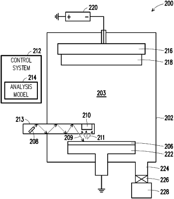
11. A system, comprising:
a thin-film deposition chamber configured to deposit a thin-film on a wafer;
a tube including:
a radiation source configured to irradiate the thin-film with excitation light;
an emissions sensor configured to detect an emission spectrum from the wafer responsive to the excitation light, wherein the tube is configured to extend partially into the thin-film deposition chamber such that the radiation source is external to the thin-film deposition chamber and the emissions sensor is within the thin-film deposition chamber; and
a control system coupled to the radiation source and the emissions sensor and configured to detect contamination of the thin-film by analyzing the emission spectrum and to stop thin-film deposition processes in the thin-film deposition chamber responsive to detecting contamination of the thin-film.
|