| CPC G01M 11/30 (2013.01) [G02B 6/12007 (2013.01); G02B 2006/12061 (2013.01); G02B 2006/12145 (2013.01); G02B 2006/12164 (2013.01)] | 20 Claims |
|
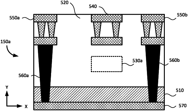
1. A system, including:
a plurality of optical devices including a first material embedded in a second material, wherein each optical device of the plurality of optical devices is associated with a different thickness range of a plurality of thickness ranges for the first material, and wherein the first material comprises a semiconductor material;
a first capacitance measurement point including the first material embedded in the second material; and
a second capacitance measurement point including a region from which the first material has been replaced with the second material.
|