US 11,684,949 B2
CMOS ultrasonic transducers and related apparatus and methods
Jonathan M. Rothberg, Miami Beach, FL (US); Keith G. Fife, Palo Alto, CA (US); Tyler S. Ralston, Clinton, CT (US); Gregory L. Charvat, Guilford, CT (US); and Nevada J. Sanchez, Guilford, CT (US)
Assigned to BFLY OPERATIONS, INC., Burlington, MA (US)
Filed by BFLY Operations, Inc., Guilford, CT (US)
Filed on Oct. 30, 2020, as Appl. No. 17/86,311.
Application 17/086,311 is a continuation of application No. 16/364,388, filed on Mar. 26, 2019, granted, now 10,843,227.
Application 16/364,388 is a continuation of application No. 15/581,511, filed on Apr. 28, 2017, granted, now 10,272,470.
Application 15/581,511 is a continuation of application No. 15/158,968, filed on May 19, 2016, granted, now 9,718,098.
Application 15/158,968 is a continuation of application No. 14/172,383, filed on Feb. 4, 2014, granted, now 9,499,392.
Claims priority of provisional application 61/760,932, filed on Feb. 5, 2013.
Claims priority of provisional application 61/760,968, filed on Feb. 5, 2013.
Claims priority of provisional application 61/760,951, filed on Feb. 5, 2013.
Claims priority of provisional application 61/760,891, filed on Feb. 5, 2013.
Prior Publication US 2021/0114060 A1, Apr. 22, 2021
This patent is subject to a terminal disclaimer.
Int. Cl. B06B 1/02 (2006.01); B81B 3/00 (2006.01); B81C 1/00 (2006.01); G10K 11/18 (2006.01); G10K 9/12 (2006.01); B81B 7/00 (2006.01)
CPC B06B 1/02 (2013.01) [B06B 1/0292 (2013.01); B81B 3/0021 (2013.01); B81B 7/0077 (2013.01); B81C 1/00158 (2013.01); G10K 9/12 (2013.01); G10K 11/18 (2013.01); B81B 2203/0127 (2013.01); B81B 2203/0315 (2013.01); B81B 2207/015 (2013.01); B81C 2201/013 (2013.01); B81C 2203/0118 (2013.01); B81C 2203/0735 (2013.01); B81C 2203/0771 (2013.01)] 10 Claims
OG exemplary drawing
 
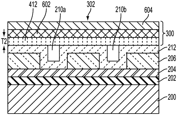
1. An ultrasound transducer device, comprising:
a first silicon substrate;
a second silicon substrate fusion-bonded to the first silicon substrate with a gap between the first silicon substrate and the second silicon substrate;
a first conductive layer formed on the first silicon substrate;
a second conductive layer formed on the first conductive layer; and
a layer of silicon dioxide formed on the second conductive layer such that the second conductive layer is disposed between the first conductive layer and the layer of silicon dioxide.