| CPC H01L 45/06 (2013.01) [G11C 13/0004 (2013.01); G11C 13/0069 (2013.01); H01L 45/144 (2013.01)] | 17 Claims |
|
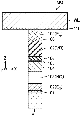
1. A semiconductor memory device comprising:
a first electrode and a second electrode;
a phase change layer disposed between the first electrode and the second electrode; and
a first layer disposed between the first electrode and the phase change layer, wherein
the phase change layer contains at least one of germanium (Ge), antimony (Sb), and tellurium (Te), and
the first layer contains:
aluminum (Al) and antimony (Sb), or
tellurium (Te) and at least one of zinc (Zn), lanthanum (La), cerium (Ce), praseodymium (Pr), neodymium (Nd), samarium (Sm), europium (Eu), gadolinium (Gd), terbium (Tb), dysprosium (Dy), holmium (Ho), erbium (Er), thulium (Tm), ytterbium (Yb), and lutetium (Lu),
wherein
the first layer contains a crystal having a first lattice constant,
the phase change layer contains a crystal having a second lattice constant, and
the first lattice constant is larger than 90% and smaller than 110% of the second lattice constant.
|