| CPC H01L 27/3209 (2013.01) [H01L 27/3211 (2013.01); H01L 27/3246 (2013.01); H01L 27/3248 (2013.01); H01L 27/3258 (2013.01); H01L 27/322 (2013.01)] | 13 Claims |
|
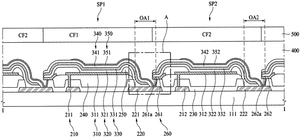
1. A display device, comprising:
a substrate including a plurality of pixels, each of the plurality of pixels including only a first sub-pixel and a second sub-pixel;
a first electrode in each of the first sub-pixel and the second sub-pixel;
a third electrode in each of the first sub-pixel and the second sub-pixel;
a second electrode between the first electrode and the third electrode;
a first light-emitting layer between the first electrode and the second electrode, the first light-emitting layer being configured to emit light of a first color;
a second light-emitting layer between the second electrode and the third electrode, the second light-emitting layer being configured to emit mixed light of second and third colors that are different from each other;
a color filter including:
a first color filter corresponding to the first sub-pixel; and
a second color filter corresponding to the second sub-pixel,
a first driving transistor in each of the first sub-pixel and the second sub-pixel, and configured to apply a first voltage to the first electrode;
a second driving transistor in each of the first sub-pixel and the second sub-pixel, and configured to apply a second voltage to the third electrode;
an insulating film on the first driving transistor and the second driving transistor, the insulating film including an opening area that partially exposes the second driving transistor; and
a mask pattern on the insulating film between the first sub-pixel and the second sub-pixel, and including a protrusion that partially covers the opening area,
wherein each of the first sub-pixel and the second sub-pixel is configured to allow the first light-emitting layer and the second light-emitting layer to emit light independently,
wherein each of the plurality of pixels is configured to emit light of at least three colors,
wherein the first color filter is configured to:
transmit the light of the first color emitted from the first light-emitting layer,
transmit the light of the second color of the mixed light emitted from the second light-emitting layer, and
block light of the third color of the mixed light emitted from the second light-emitting layer,
wherein the second color filter is configured to:
transmit the light of the third color of the mixed light emitted from the second light-emitting layer, and
block light of the second color of the mixed light emitted from the second light-emitting layer,
wherein the third electrode directly contacts the second driving transistor below the mask pattern in the opening area,
wherein the mask pattern and the third electrode are provided on different layers,
wherein a surface of the protrusion of the mask pattern facing away from the first light-emitting layer faces toward the substrate, and
wherein the first light-emitting layer directly contacts an upper surface of the protrusion of the mask pattern in the second sub-pixel.
|