| CPC H10K 59/131 (2023.02) [G06V 40/13 (2022.01); H10K 59/65 (2023.02); H10K 71/00 (2023.02); H10K 59/1201 (2023.02)] | 17 Claims |
|
1. An array substrate, comprising:
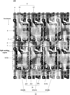
a plurality of pixel units in an array, wherein each of the plurality of pixel units comprises a plurality of sub-pixel units, and each of the plurality of sub-pixel units comprises a light emitting region and a non-light emitting region;
a light emitting element, wherein each of the plurality of sub-pixel units comprises the light emitting element, the light emitting element comprises a light emitting layer and a first electrode electrically connected to the light emitting layer, and at least a part of the first electrode is in the light emitting region; and
a plurality of first wires which are configured to supply a power signal to the light emitting element and comprise a first sub-wire, wherein the first sub-wire extends along a first direction and comprises a plurality of portions, the plurality of portions are arranged in the first direction, adjacent two portions of the plurality of portions are disconnected and spaced apart from each other so that the first sub-wire has an opening provided between the adjacent two portions of the plurality of portions, and the opening is in the light emitting region,
wherein the first electrode of the light emitting element is stacked with the plurality of first wires in a direction perpendicular to the array substrate, and at least a part of an orthographic projection of the opening on the array substrate does not overlap with an orthographic projection of the first electrode on the array substrate,
wherein the array substrate further comprises a plurality of auxiliary wires extending along a second direction intersecting the first direction, the plurality of first wires further comprise a second sub-wire continuously extending along the first direction, and the plurality of portions of the first sub-wire are respectively electrically connected to the second sub-wire through the plurality of auxiliary wires, and
wherein the plurality of first wires comprise a plurality of the second sub-wires, and at least one of the plurality of portions of the first sub-wire is electrically connected to one second sub-wire, which is closest to the at least one of the plurality of portions of the first sub-wire, of the plurality of second sub-wires through at least one of the plurality of auxiliary wires.
|