| CPC H10K 59/126 (2023.02) [H01L 29/7869 (2013.01); H01L 29/78672 (2013.01); H10K 71/00 (2023.02)] | 18 Claims |
|
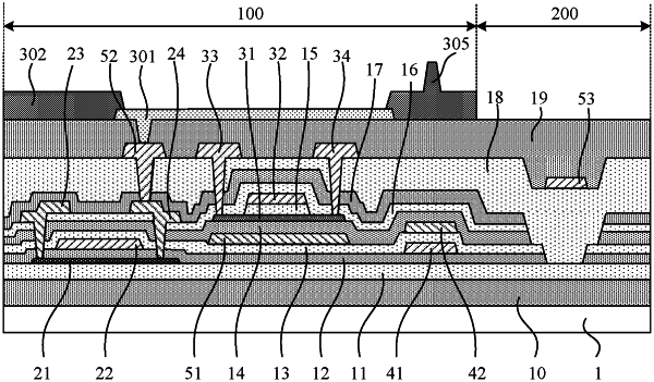
1. A display substrate, comprising: a substrate, an active structure layer disposed on the substrate, a first source-drain structure layer disposed on a side of the active structure layer away from the substrate, and a second source-drain structure layer disposed on a side of the first source-drain structure layer away from the substrate; wherein
the active structure layer comprises a first active layer and a second active layer;
the first source-drain structure layer comprises a first active via and a first source-drain electrode, and the first source-drain electrode is connected to the first active layer through the first active via; and
the second source-drain structure layer comprises a second active via and a second source-drain electrode, and the second source-drain electrode is connected to the second active layer through the second active via;
wherein the second source-drain structure layer comprises:
a seventh insulating layer covering the first source-drain structure layer, wherein a second via is formed on the seventh insulating layer, and an insulating layer covering the second active layer is reserved in the second via;
a first planarization layer disposed on a side of the seventh insulating layer away from the substrate, wherein after a fourth via is formed communicated to the second via on the first planarization layer, the insulating layer in the second via is etched to form the second active via
a second source electrode and a second drain electrode disposed on a side of the seventh insulating layer away from the substrate; wherein the second source electrode and the second drain electrode are both connected to the second active layer through the second active via.
|