| CPC H10K 59/123 (2023.02) [G02F 1/0063 (2013.01); G02F 2203/02 (2013.01); G02F 2203/22 (2013.01)] | 15 Claims |
|
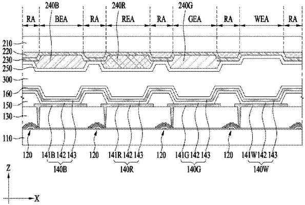
1. A display device comprising:
a lower substrate and an upper substrate opposite the lower substrate;
a lower electrode on the lower substrate;
a bank insulating layer on the lower substrate, the bank insulating layer covering an edge of the lower electrode;
a light-emitting layer on a surface of the lower electrode exposed by the bank insulating layer;
an upper electrode on the light-emitting layer;
a reflective pattern on the upper substrate, the reflective pattern overlapping with the bank insulating layer; and
a half-mirror layer disposed side by side with the reflective pattern on the upper substrate, the half-mirror layer overlapping with a surface of the upper substrate exposed by the reflective pattern,
wherein an edge of the half-mirror layer overlaps with the reflective pattern.
|