| CPC H05K 1/0268 (2013.01) [H05K 2201/0776 (2013.01); H05K 2201/09627 (2013.01); H05K 2201/09663 (2013.01); H05K 2201/09672 (2013.01)] | 10 Claims |
|
1. A method for controlling a quality of metallization of a printed circuit with multiple layers comprising an upper layer and a lower layer sandwiching at least one intermediate layer, each layer having a track made of conductive material and through-holes referred to as vias that are provided with an inner peripheral wall suitable for being coated with a metal border in a step of metallizing the printed circuit, the method comprising:
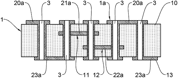
producing a control circuit including n vias, with n being an integer greater than or equal to three, that are connected electrically in series between two electrical terminals, so that an electric current applied between said electrical terminals passes at least partially through each one of the n vias in the direction of its height,
applying a current of defined intensity between the two electrical terminals of the control circuit,
measuring the corresponding potential difference, and
comparing the measured value with a threshold value representative of the potential difference so as to validate the printed circuit when the measured value is lower than the threshold value,
wherein the control circuit is configured to pass through at least a portion of a track of each one of the layers of the printed circuit, each one of the n vias connecting a track portion of one layer to a track portion of another layer, the threshold value being representative of a potential difference obtained for:
n vias of the control circuit that are provided with a metal border of predefined minimum thickness deposited on a peripheral wall of each via between the two layers that the via connects,
an alignment of the metal border located at each layer with the track portion on the layer, and
a minimum thickness of metallization of the track portions on each one of the layers of the control circuit,
wherein the printed circuit comprises at least three superposed layers including the upper layer, the lower layer, and the intermediate layer.
|