| CPC H03K 19/17744 (2013.01) [H01L 27/0688 (2013.01)] | 16 Claims |
|
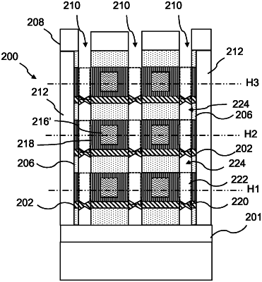
1. A method for forming a 3D integrated circuit comprising a stack of logic cells, each logic cell forming part of one of a plurality of device tiers of the 3D integrated circuit, the method comprising:
patterning a layer stack comprising, for each device tier, in a bottom-up direction, a single active semiconductor layer, a sacrificial layer and an interlayer-dielectric layer, the patterning comprising forming trenches in the layer stack, and wherein the layer stack by the patterning is partitioned into a plurality of sub-stacks comprising, for each device tier, an active semiconductor layer portion, a sacrificial layer portion and an inter-layer dielectric portion;
removing the sacrificial layer portions in each device tier of each sub-stack;
forming a gate stack in spaces formed by removing the sacrificial layer portions, the gate stack comprising a gate dielectric and gate electrode material forming gate lines;
recessing the gate lines from the trenches to form cavities on each side of each recessed gate line;
depositing a spacer material in said cavities to form spacers along each recessed gate line; and
forming source/drain regions on end surfaces of the active semiconductor layer portions facing the trenches.
|