| CPC H03K 17/04106 (2013.01) [H03K 17/063 (2013.01); H03K 17/102 (2013.01); H03K 17/693 (2013.01)] | 27 Claims |
|
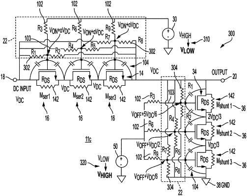
1. An apparatus comprising:
a stacked switch comprising a plurality of series-connected switches from a first switch to a last switch, each switch of the plurality of series-connected switches having a gate terminal, a source terminal, and a drain terminal; and
a passive gate bias network electrically connected to the drain terminal of the first switch of the plurality of series-connected switches and the gate terminals of the plurality of series-connected switches, and configured to successively reduce, from the first switch to the last switch, a voltage applied to respective gate terminals of the plurality of series-connected switches,
wherein the passive gate bias network comprises:
a voltage divider comprising first and second resistors and a midpoint electrically connecting the first and second resistors to one another and to the gate terminal of a switch of the plurality of series-connected switches; and
a gate bias path that bypasses each of the first and second resistors of the voltage divider to bias the gate terminal via the midpoint of the voltage divider.
|