| CPC H03F 3/45192 (2013.01) [H04L 12/40 (2013.01); H03F 2200/78 (2013.01); H03F 2203/30061 (2013.01); H03F 2203/45508 (2013.01); H04L 2012/40215 (2013.01)] | 10 Claims |
|
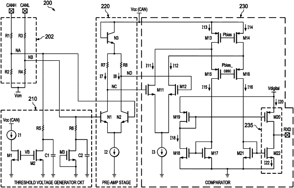
1. A circuit, comprising:
a pre-amplifier stage having first and second outputs;
a comparator having first and second inputs, the first input coupled to the first output of the pre-amplifier stage, and the second input coupled to the second output of the pre-amplifier stage, the comparator including:
an input differential transistor pair wherein the differential transistor pair comprises:
a first metal oxide field effect transistor (MOSFET) having a gate, a drain and a source wherein the gate of the first MOSFET is directly coupled to the first input of the comparator; and
a second (MOSFET) having a gate, a drain and a source wherein the gate of the second MOSFET is directly coupled to the second input of the comparator; and
a second pair of transistors in a cascode configuration wherein the second pair of transistors comprises:
a third MOSFET haying a gate, a drain and a source wherein the source of the third MOSFET is directly coupled to the drain of the first MOSFET; and
a fourth MOSFET haying a gate, a drain and a source wherein the source of the fourth MOSFET is directly coupled to the drain of the second MOSFET; and
a push-pull output stage wherein the push-pull output stage comprises:
a fifth MOSFET haying a gate, a drain and a source; and
a sixth MOSFET haying a gate, a drain and a source wherein the gate of the sixth transistor is directly coupled to the drain of the fourth transistor, and the drain of the sixth transistor is directly coupled to the drain of the fifth transistor.
|