| CPC H01L 33/504 (2013.01) [G02B 1/005 (2013.01); H01L 25/0753 (2013.01); H01L 33/50 (2013.01); H01L 33/60 (2013.01); G02B 6/1225 (2013.01); H01L 2933/0041 (2013.01); H01L 2933/0058 (2013.01); H01L 2933/0083 (2013.01)] | 13 Claims |
|
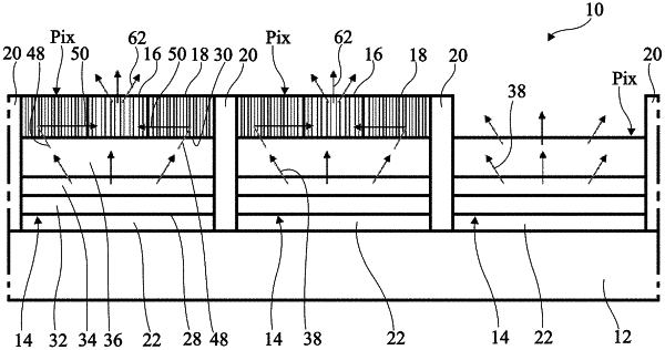
1. An optoelectronic device comprising:
light-emitting sources, each light-emitting source being capable of emitting a first radiation at a first wavelength and comprising first and second opposite surfaces;
photoluminescent blocks distributed into first photoluminescent blocks capable of converting by optical pumping the first radiation into a second radiation at a second wavelength and second photoluminescent blocks capable of converting by optical pumping the first radiation into a third radiation at a third wavelength; and
for each photoluminescent block, an optical coupler comprising a first photonic crystal at least partially surrounding said photoluminescent block, both photonic crystal and photoluminescent block covering the first surface of one of the light-emitting sources, the photonic crystal and the photoluminescent block being the one next to the other on said first surface, both the photonic crystal and the photoluminescent block being in contact with said first surface, the optical coupler being capable of modifying the propagation direction of rays of the first radiation emitted by said light-emitting source to redirect the rays towards said photoluminescent block.
|