| CPC H01L 31/115 (2013.01) [H01L 21/0243 (2013.01); H01L 21/0254 (2013.01); H01L 21/0262 (2013.01); H01L 21/02433 (2013.01); H01L 21/02458 (2013.01); H01L 21/02562 (2013.01); H01L 31/03044 (2013.01); H01L 31/0384 (2013.01); H01L 31/184 (2013.01); H01L 31/1856 (2013.01); Y02E 10/544 (2013.01)] | 8 Claims |
|
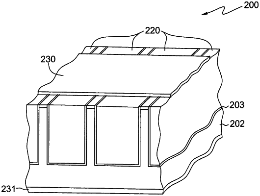
1. A method of fabricating a radiation-detecting structure, the method comprising:
providing a substrate, the substrate comprising at least one mask formed on an upper surface of the substrate and at least one trench defined by a first sidewall and a second sidewall extending into the substrate from the upper surface, the at least one trench having a width measured between the first sidewall and the second sidewall and a vertical height that is at least five times greater than the width as measured along the first sidewall and the second sidewall, the first and second sidewalls each having at least one vertical (111) surface patterned thereon;
epitaxially growing a radiation-responsive semiconductor material layer from both the first sidewall and the second sidewall of the at least one trench of the substrate such that the radiation-responsive semiconductor material layer fills the at least one trench without extending outwards from the at least one trench past the at least one mask, the radiation-responsive semiconductor layer comprising a layer of hexagonal boron nitride, the epitaxially growing comprises growing the hexagonal boron nitride layer with an a-axis thereof aligned parallel to the at least one vertical (111) surface of the first sidewall and second sidewall of the at least one trench of the substrate, the radiation-responsive semiconductor material layer is responsive to incident radiation by generating and collecting charge carriers therein; and
providing a first contact structure above the substrate and a second contact structure below the substrate, the first contact structure being positioned over the at least one trench and spanning at least the width of the at least one trench, the first and second contact structures being in electrical contact with the radiation-responsive semiconductor material layer and facilitating detecting the incident radiation by collecting the charge carriers generated within the radiation- responsive semiconductor material layer due to the incident radiation.
|