| CPC H01L 31/09 (2013.01) [H01L 31/028 (2013.01); H01L 31/0216 (2013.01); H01L 31/022475 (2013.01); H01L 31/143 (2013.01); H01L 31/1804 (2013.01); H01L 31/1884 (2013.01)] | 23 Claims |
|
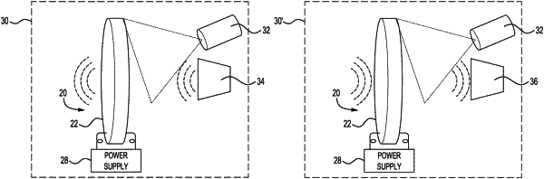
1. A photoconductor assembly comprising:
a substrate formed of an undoped and single-crystal semiconductor material that is configured to reflect or absorb electromagnetic energy;
a plurality of electrodes arranged normal to the substrate;
a power supply that applies a voltage to the electrodes for modulating the electromagnetic energy through the substrate; and
a light source that generates excitation wavelengths for illuminating the substrate having energies that are equal to or greater than a band gap energy of the semiconductor material;
wherein the plurality of electrodes are arranged on opposing sides of the substrate; and
wherein the power supply is used to electrically bias the substrate and reduce a recombination rate of relevant carriers by increasing radio frequency modulation.
|