| CPC H01L 31/0687 (2013.01) [H01L 31/02363 (2013.01); H01L 31/022425 (2013.01); H01L 31/022433 (2013.01); H01L 31/03529 (2013.01); H01L 31/035218 (2013.01); H01L 31/035227 (2013.01); H01L 31/043 (2014.12); H01L 31/0543 (2014.12); H01L 31/0547 (2014.12); H01L 31/075 (2013.01); H01L 31/076 (2013.01); Y02E 10/52 (2013.01); Y02E 10/544 (2013.01); Y02E 10/548 (2013.01)] | 18 Claims |
|
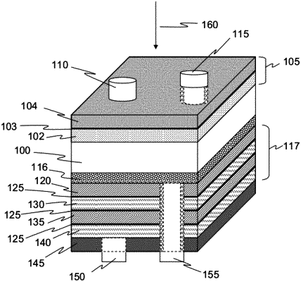
1. An energy harvester configured to harvest energy during both day and night, comprising:
a substrate formed from a non-electrically conductive material, wherein the substrate has a first surface and a second surface;
a first electrode;
a second electrode;
a solar harvester on the first surface of the substrate and electrically connected between the first and second electrodes, comprising
at least one first p-n or p-i-n junction formed on or into the substrate, wherein the at least one first p-n or p-i-n junction comprising cutoff wavelengths between 0.3 μm to 2.5 μm;
wherein the second electrode being in contact to a n or a p layer forming the at least one first p-n or p-i-n junction and insulated from a conductive material that encircles the second electrode;
a buffer layer directly attached to the second surface of the substrate, wherein the buffer layer comprises a semiconductor material from a group consisting of CdZnTe, HgCdTe, HgZnTe, ZnS, CdS, CdTe, ZnSe, CdSe and combinations thereof;
a third electrode;
a fourth electrode; and
a thermal harvester attached to the buffer layer and electrically connected between the third and fourth electrodes, comprising
a absorption layer attached to the buffer layer, comprising
a first material of p or n type layer; and
a second material of n or p type layer,
wherein the first and the second material layers forming at least one second p-i-n junction with an additional intrinsic or low doped material layer in between the first and second material layers and providing an open circuit voltage and the at least one second p-i-n junction comprising
cutoff wavelengths between 2 μm to 40 μm, and
wherein the energy harvester is monolithic.
|