| CPC H01L 29/78391 (2014.09) [H01L 27/0705 (2013.01); H01L 29/40111 (2019.08); H01L 29/516 (2013.01); H01L 29/517 (2013.01); H01L 29/6684 (2013.01)] | 23 Claims |

|
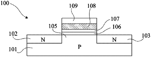
1. A method of manufacturing a first transistor and a second transistor on a semiconductor substrate, the method comprising:
depositing an interface layer on the semiconductor substrate, the interface layer comprising silicon oxynitride;
depositing a gate insulator layer on the interface layer;
depositing a first ferroelectric layer on the gate insulator layer over a first region of the semiconductor substrate for the first transistor;
during a same deposition step, depositing a metal gate layer on the gate insulator layer over a second region of the semiconductor substrate for the second transistor and on the first ferroelectric layer over the first region of the semiconductor substrate for the first transistor; and
patterning the metal gate layer, first ferroelectric layer, gate insulator layer and interface layer to form a first gate stack for the first transistor which includes the metal gate layer, first ferroelectric layer, gate insulator layer and interface layer and a second gate stack for the second transistor which includes the metal gate layer, gate insulator layer and interface layer.
|