| CPC H01L 29/66977 (2013.01) [G06N 10/00 (2019.01); H01L 21/823475 (2013.01); H01L 27/088 (2013.01); H01L 27/1203 (2013.01); H01L 29/158 (2013.01); H01L 29/66984 (2013.01); H01L 29/7831 (2013.01); H01L 29/82 (2013.01); H01L 29/437 (2013.01)] | 24 Claims |
|
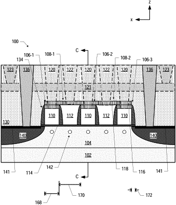
1. A quantum dot device, comprising:
a substrate, wherein the substrate includes (111) silicon;
a quantum well stack on the substrate, wherein the quantum well stack includes a quantum well layer that includes (111) germanium;
a first doped region in a first portion of the quantum well stack;
a second doped region in a second portion of the quantum well stack;
a continuous portion of the quantum well stack between the first doped region and the second doped region, wherein a dopant concentration of the continuous portion of the quantum well stack between the first doped region and the second doped region is lower than a dopant concentration of the first doped region and a dopant concentration of the second doped region; and
a plurality of gates above the continuous portion of the quantum well stack between the first doped region and the second doped region, wherein the quantum well layer is between the plurality of gates and the substrate.
|