| CPC H01L 29/1054 (2013.01) [H01L 21/823807 (2013.01); H01L 21/823821 (2013.01); H01L 27/0924 (2013.01); H01L 29/66795 (2013.01); H01L 29/785 (2013.01); H01L 29/7848 (2013.01); H01L 29/165 (2013.01)] | 20 Claims |
|
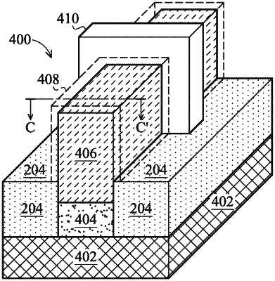
1. A semiconductor device comprising:
a substrate;
a fin structure disposed over the substrate, wherein a total length of the fin structure is along a first direction, a total width of the fin structure is along a second direction that is substantially perpendicular to the first direction, the total width is a channel width of a channel region of the fin structure, the total length of the fin structure is at least 100 nm, and a ratio of the total width of the fin structure to the total length of the fin structure is about 1:5 to about 1:10, and further wherein the fin structure includes:
a first silicon epitaxial layer disposed directly on the substrate, wherein the first silicon epitaxial layer extends the total length of the fin structure,
a silicon germanium epitaxial layer disposed directly on the first silicon epitaxial layer, wherein the silicon germanium epitaxial layer extends the total length of the fin structure and includes relaxed silicon germanium, and
a second silicon epitaxial layer disposed directly on the silicon germanium epitaxial layer, wherein the second silicon epitaxial layer extends the total length of the fin structure, the second silicon epitaxial layer includes strained silicon, the second silicon epitaxial layer includes a longitudinal tensile stress component and a relaxed transversal stress component, the longitudinal tensile stress component is along the first direction, and the relaxed transversal stress component is along the second direction;
a gate structure disposed on the channel region of the fin structure, such that the gate structure interposes a source region and a drain region of the fin structure, wherein the channel region, the source region, and the drain region each include the first silicon epitaxial layer, the silicon germanium epitaxial layer, and the second silicon epitaxial layer of the fin structure; and
wherein:
in the source region and the drain region, the silicon germanium epitaxial layer has a first sidewall, a second sidewall, a top, and a bottom configured to provide the silicon germanium epitaxial layer with a rectangular shape,
upper portions of the first sidewall and the second sidewall of the silicon germanium epitaxial layer are completely covered and physically contacted by the second silicon epitaxial layer and lower portions of the first sidewall and the second sidewall of the silicon germanium epitaxial layer are completely covered and physically contacted by a substrate isolation structure, and
a width of the silicon germanium epitaxial layer along the second direction is substantially uniform above a top of the substrate isolation structure and the substrate isolation structure physically contacts a top surface of the substrate.
|