| CPC H01L 29/0653 (2013.01) [H01L 29/0847 (2013.01); H01L 29/1083 (2013.01); H01Q 1/2283 (2013.01)] | 14 Claims |
|
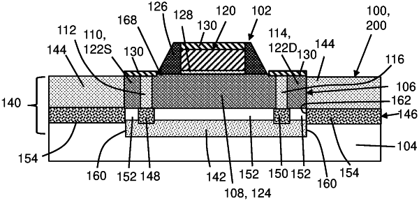
1. An integrated circuit (IC) structure, comprising:
an active device over a bulk semiconductor substrate, the active device including a semiconductor layer having a center region, a first end region laterally spaced from the center region by a first trench isolation, a second end region laterally spaced from the center region by a second trench isolation, a gate over the center region, and a source/drain region in each of the first and second end regions; and
an isolation structure around the active device in the bulk semiconductor substrate, the isolation structure including:
a polycrystalline isolation layer under the active device,
a third trench isolation around the active device, and
a porous semiconductor layer between the first trench isolation and the polycrystalline isolation layer and between the second trench isolation and the polycrystalline isolation layer.
|