| CPC H01L 27/1446 (2013.01) [H01L 31/0203 (2013.01); H01L 31/02005 (2013.01); H01L 31/02019 (2013.01); H01L 31/035281 (2013.01); H01L 31/105 (2013.01)] | 19 Claims |
|
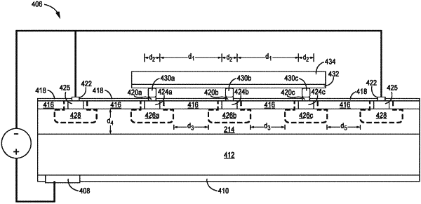
1. A PIN photodetector comprising:
a first semiconductor layer;
a second semiconductor cap layer;
an array of semiconductor regions located within the second semiconductor cap layer, wherein each of the semiconductor regions in the array are separated from one another by approximately the same distance d1;
an absorber layer located between the first semiconductor layer and the second semiconductor cap layer including the of semiconductor regions; and
wherein one or more electrical responses are generated by the array of semiconductor regions in response to light incident to the PIN photodetector.
|