| CPC H01L 27/11807 (2013.01) [H01L 21/76816 (2013.01); H01L 23/5226 (2013.01); H01L 27/0207 (2013.01); H01L 27/1052 (2013.01); H01L 27/11 (2013.01); H01L 2027/11861 (2013.01); H01L 2027/11866 (2013.01); H01L 2027/11875 (2013.01); H01L 2027/11885 (2013.01)] | 10 Claims |
|
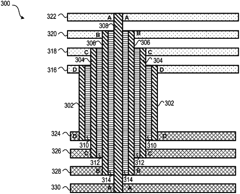
1. A method for forming a semiconductor device, comprising:
forming a first opening in a dielectric stack over a substrate, the first opening has a cylinder shape with a first sidewall and a first bottom;
depositing a first conductive layer along the first sidewall of the first opening and a first insulating layer along an inner sidewall of the first conductive layer so that the first conductive layer and the first insulating layer having closed-shape and concentrically arranged, a bottom of the first conductive layer and a bottom of the first insulating layer being positioned on the first bottom of the first opening;
etching the dielectric stack along an inner sidewall of the first insulating layer so as to form a second opening, the second opening extending into the dielectric stack and having a second sidewall and a second bottom, the second sidewall being formed along the inner sidewall of the first insulating layer and further extending into the dielectric stack, the second bottom of the second opening being positioned below the bottoms of the first conductive layer and first insulating layer; and
depositing a second conductive layer along the second sidewall of the second opening and a second insulating layer along an inner sidewall of the second conductive layer, a bottom of the second conductive layer and a bottom of the second insulating layer being positioned on the second bottom of the second opening so that the bottom of the second conductive layer is positioned below the bottom of the first conductive layer to form a staggered configuration.
|