| CPC H01L 27/0924 (2013.01) [H01L 21/3086 (2013.01); H01L 29/0673 (2013.01); H01L 29/0847 (2013.01); H01L 29/1033 (2013.01); H01L 29/165 (2013.01); H01L 29/41791 (2013.01); H01L 29/4232 (2013.01); H01L 29/517 (2013.01); H01L 29/6681 (2013.01); H01L 29/66545 (2013.01); H01L 29/785 (2013.01); H03K 19/20 (2013.01)] | 22 Claims |
|
1. A semiconductor device comprising:
a substrate;
a buffer layer that is compositionally distinct from the substrate;
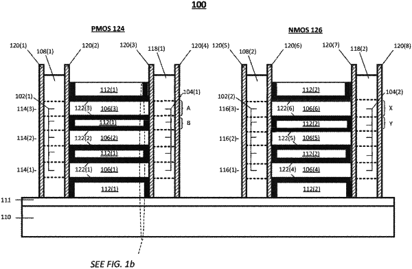
a plurality of strained n-type nanowires above said buffer layer, wherein immediately neighboring ones of the plurality of strained n-type nanowires are separated by a first vertical distance;
a first gate structure wrapped around said plurality of strained n-type nanowires;
a first common source or drain structure at a first side of the first gate structure, the first common source or drain structure in contact with a first lateral end of each of the plurality of strained n-type nanowires;
a second common source or drain structure at a second side of the first gate structure, the second common source or drain structure in contact with a second lateral end of each of the plurality of strained n-type nanowires;
a plurality of strained p-type nanowires above said buffer layer, wherein immediately neighboring ones of the plurality of strained p-type nanowires are separated by a second vertical distance different than the first vertical distance, and wherein an uppermost one of the plurality of strained p-type nanowires has an uppermost surface co-planar with an uppermost surface of an uppermost one of the plurality of strained n-type nanowires;
a second gate structure wrapped around said plurality of strained p-type nanowires;
a third common source or drain structure at a first side of the second gate structure, the third common source or drain structure in contact with a first lateral end of each of the plurality of strained p-type nanowires;
a fourth common source or drain structure at a second side of the second gate structure, the fourth common source or drain structure in contact with a second lateral end of each of the plurality of strained p-type nanowires; and
a plurality of spacers disposed on sidewalls of the first and second gate structures, each of the plurality of spacers wraps around the first, second, third and fourth common source or drain structures respectively.
|